about Audio, High Fidelity
& Home Entertainment technologies
pid: 636-2026/04/22 (v1.2)
Privacy Policy

HD25 lab evaluation included measurements using the coaxial input and with 96kHz and 176.4kHz sample rate signals. Generally speaking, it seems that the converter has no significant changes in performance related to the sample rate.
The digital interface of HD25 proved to be able to sufficiently suppress incoming jitter. The corresponding curve stayed around -60dB for an 80nS pp injected jitter signal and around -70dB for 215nS pp jitter, the later being the value which corresponds to a limit above which the input of the converter ceases to remain locked to the source. This performance is very good and justifies the strategy used by Hegel regarding incoming signal jitter attenuation (either associated with the SRC, or not).
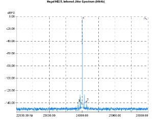
Jitter introduced by the device itself was also very low with estimates ranging between 26pS (based on findings close to 60Hz) and 7.7pS (for sidebands above 100Hz).
Jitter attenuation. Signal jitter 80nS pp, (purple curve), 215ns pp (pink), S/PDIF input.
Inferred jitter spectrum. Input Signal : 24kHz/-5dBFS.
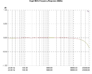
Frequency response is, as expected, flat with a just visible cut-off trend above 10kHz, with no more than the 0.5dBr difference compared to the mid-band, for frequencies above 40kHz. Channel balance is exemplary.
Transition and stop-band response of the filters used are typical with the slope decreasing with sample rate, as expected. Hegel has selected a rather "conservative" response in case of 176.4kHz rate, where the cutoff frequency is in the same area as that of the 96k sample rate but the slope is clearly softer. The stop-band is generally smooth.
Frequency response (96kHz/24bit).
Low pass filter response. 44.1kHz (orange curve), 96kHz (violet), 176.4kHz (blue).
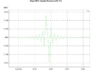
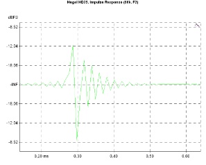
The two user-selectable digital filters (F1 and F2) have no significant differences in the frequency domain (therefore the corresponding responses are not published here), but have some differences in the time domain, the F1 showing clearly more pre-ringing compared to F2.
Time domain (impulse) response with the F1 filter.
Time domain (impulse) response with the F2 filter.
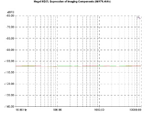
In any case, HD25 filters seem to work as intended. The relevant graph, showing -indirectly- the ability to suppress the by-products of the sampling frequency is systematically below -100dBFS.
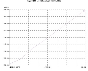
Level linearity was excellent. The relative curve remains very close to the ideal levels down to -120dBFS, both for 96kHz and 176.4kHz signals with some visible deviation making its appearance near -125dBFS. This performance ranks HD25 as one of the most level-linear converters we had the opportunity to evaluate recently. Pay attention that this diagram has a higher resolution than usual (5dBFS/Div).
Suppression of imaging components (in-band). Sample rate 96kHz (green curve), 176.4kHz (red).
Output level linearity. Signal frequency 1kHz, S/PDIF input, 96kHz (purple curve), 176.4kHz (pink).
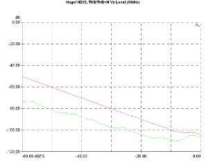
Harmonic distortion Vs frequency measurements confirm the impression one gets in terms of device performance at very low levels. Total harmonic distortion (THD) is considerably lower than -70dB for a -60dBFS signal level while THD+N was about 20dB higher. Near the converter's maximum output there are no traces of overload, an indication that the analog stage offers adequate headroom near 0dBFS.
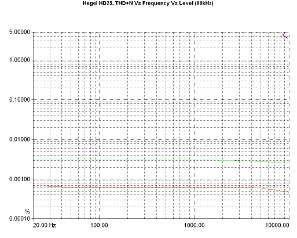
THD+N at high output levels remains around and below 0.0006%, quite close to the performance figures published by Hegel. For lower output levels (-20dBFS), THD+N was close to 0.003%. Performance changes in function with frequency are very small, with a mild downward trend at high frequency signals and minimal increase at lows when measured at high output level.
THD and THD+N Vs level. Sample rate 96kHz, THD+N (red curve), THD (green).
THD+N Vs Frequency. Sample rate 96kHz. Signal Level: -1dBFS (red curve), -20dBFS (green).
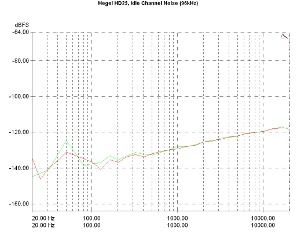
The HD25 has proved to be a rather quiet piece of equipment. Idling channel noise spectrum was below -120dBFS (up to about 10kHz) and slightly higher in the region between 10kHz and 20kHz.
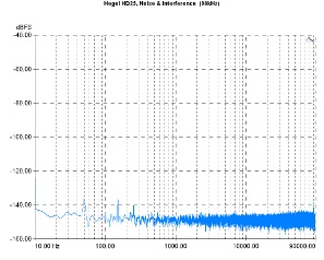
Noise measurements were very close to -100dBu (-99dBu to be precise) for the 22Hz-22kHz range and remained below -90dBu for a wider bandwidth (-93dBu/2Hz-96kHz). Out-of-band noise (>22kHz) was about -94dBu.
These values are well reflected in the relevant wide band noise spectrum, up to 96kHz.
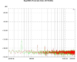
Power supply seems to have no significant negative impact on performance. The relevant spectrum (with 96kHz signals) includes some hum components (at 50/100Hz and some intermodulation products too) but all these are under the -120dBV, a figure that translates into voltages not exceeding 1.6uVrms per noise component. A quite interesting finding here is that the best behavior was reached with 176.4kHz signals, with the 50Hz component obviously weaker. It is not clear whether we are dealing with some measurement interaction here, but two slightly different methods both showed lower power line related noise in the case of the higher sample rate.
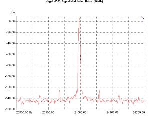
Signal modulation appears to be very low in the wide band measurement, with some components just below 30kHz (at about -110dBFS level).
Power line related noise components (2kHz bandwidth), 96kHz (green curve), 176.4kHz (red).
Modulation signal from noise (wide band). Reference signal: 24kHz.
Signal modulation noise measurement with very high frequency resolution (50Hz/Div) discloses two components close to 60Hz (probably corresponding with some jitter findings) and traces of very low intermodulation frequencies (near 7Hz).
Channel cross-talk was at typically good levels remaining near -120dB for low frequency signals and displaying a clear upward trend above 1kHz (a behavior more prominent at the right channel). Near the 20kHz limit of this measurement the worst figure we got was near -90dB.


